Nano Semiconductor Applications

Nano Semiconductor Applications

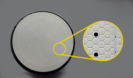
Vacuum brazed ESC base,Mutizone heater ESC,Thin film coated ceramic ESC,Vacuum brazed metal heater

  • Features
    • Multi layers enclosed with He/cooling channel
    • Spray Al2O3/W sandwich structure、mono or Bi polar ESC
    • Electrode: Break down>5000VDC
    • Flexible special surface emboss pattern and He groove engraving to improve de-chuck or minimum contact performance

Advanced Packaging Applications

Semiconductor / LED / III-V

  • Features
    • Spray Al2O3/W sandwich structure、Bi-polar ESC
    • Electrode-Break down>6000VDC
    • Optimized Electrode for chucking force enhancing
    • Applied to TSV Etching process
  • Features
    • Spray Al2O3/W sandwich structure、Bi-polar ESC
    • Max Temp <300oC

Automation Applications

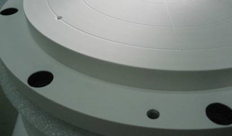
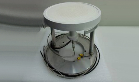
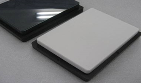
Customization based on customer requirement, for thin objects handling, materials including wafers, glass, fibers, plastic films…

  • Features
    • Spray Al2O3/W sandwich structure、Bi polar ESC
    • With doped Dielectric JR ceramic top layer
    • Operating voltage<2000VDV
    • Customized size and shape for different automation applications
    • Can be used both in atmosphere and vacuum environment
    • +/- 2000V power supply、RS232 or Digital I/O controllable
  • Features
    • Provide the capability of clamping various materials including conductor/semi-conductor/insulator
    • Can handle porous materials (fabrics/lead frame…) flexible materials (glass/copper foil…) and creatures for developing automated handling systems

A Portable Electro Static Chucking Solution